Circuit Library › RX front ends › rf-amp
Common-Gate J310 RF Amplifier
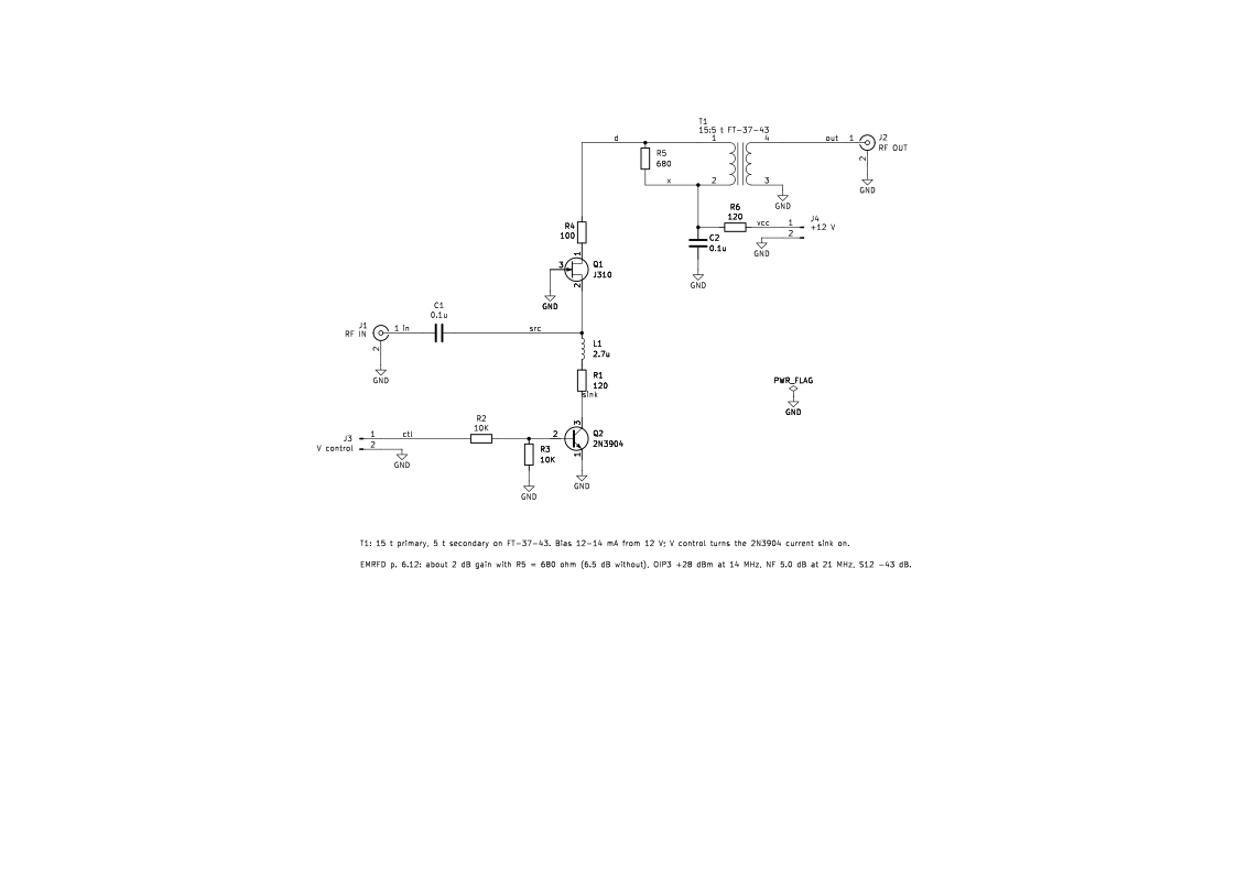
Bench sheet (PDF)Schematic PDFSPICE netlist (.cir)KiCad project (.zip)
- gain_db 2 book
- oip3_dbm 28 at 14 MHz book
- nf_db 5.0 at 21 MHz book
- s12_db -43 book
- gain_db 2.0 at 14 MHz simulated
- rl_db 13.9 at 14 MHz simulated
What it does
A low-gain, high-intercept RF amplifier for a receiver front end, with good reverse isolation (S12 about −43 dB). It keeps LO leakage off the antenna.
How it works
The J310 runs common gate, so its source presents a near-50 Ω input. A control voltage sets the drain current; the simulation shows current turning on above about 1.5 V and 13.6 mA at 2.0 V. T1 matches the drain to the 50 Ω output. R5 = 680 Ω loads the output for about 2 dB gain; omit it for about 6.5 dB (EMRFD p. 6.12).
Building it
- Check the J310 pinout against your part's datasheet; the schematic pinout is unverified.
- Adjust the control voltage for 12–14 mA drain current.
Tuning and testing
Measure drain current first. Then check gain and return loss with a signal generator and a return-loss bridge.
Where it comes from
A front-end amplifier from Experimental Methods in RF Design, Chapter 6.
Simulation
Simulated in ngspice from the schematic netlist. Not a measurement.
Parts list
| Ref | Value | Qty |
|---|---|---|
| C1,C2 | 0.1u | 2 |
| J1 | RF IN | 1 |
| J2 | RF OUT | 1 |
| J3 | V control | 1 |
| J4 | +12 V | 1 |
| L1 | 2.7u | 1 |
| Q1 | J310 | 1 |
| Q2 | 2N3904 | 1 |
| R1,R6 | 120 | 2 |
| R2,R3 | 10K | 2 |
| R4 | 100 | 1 |
| R5 | 680 | 1 |
| T1 | 15:5 t FT-37-43 | 1 |
SPICE netlist
References
- EMRFD Fig 6.32, p. 6.12